How to Design a DC-DC Buck Converter?
Designing a DC-DC buck converter is an essential skill for electrical engineers and electronics enthusiasts. A buck converter is a type of DC-DC converter that steps down voltage levels from a higher input voltage to a lower output voltage, making it an efficient and cost-effective way to power electronic devices. In this article, we will discuss the key steps and considerations involved in designing a DC-DC buck converter.
Step 1: Determine Your Requirements
The first step in designing a DC-DC buck converter is to determine your requirements. You need to know the input voltage range, output voltage, output current, efficiency, and other specifications of your application. These requirements will guide you in selecting the right components and designing the converter circuit.
Step 2: Select Components
Once you have determined your requirements, the next step is to select the components for your buck converter. The key components include an inductor, a capacitor, a diode, and a switch (usually a MOSFET). It is essential to choose components that can handle the input and output voltage levels, current, and power requirements of your application.
Step 3: Design the Circuit
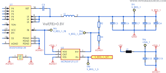
After selecting the components, you can start designing the circuit for your buck converter. The circuit typically consists of a switch, an inductor, a capacitor, and a diode arranged in a specific configuration. You will need to calculate component values, such as the inductor and capacitor values, to ensure proper operation of the buck converter.
Step 4: Simulate and Test
Before building the buck converter circuit, it is essential to simulate the circuit using simulation software such as LTspice. Simulation allows you to verify that the circuit operates as intended and to identify any potential issues. After simulation, you can prototype the circuit and conduct thorough testing to ensure that it meets your requirements.
Step 5: Optimize and Improve
Once you have tested the buck converter circuit, you may need to optimize and improve its performance. This could involve adjusting component values, switching frequencies, or feedback mechanisms to achieve better efficiency, stability, or other desired characteristics. Continuous optimization is key to creating a successful buck converter design.
Step 6: Finalize the Design
After optimizing the circuit and ensuring that it meets all requirements, you can finalize the design of your DC-DC buck converter. Document the design, including component values, schematics, and PCB layout, for future reference. Make any necessary adjustments and refinements to the circuit before proceeding to production.
Conclusion
Designing a DC-DC buck converter requires careful planning, component selection, circuit design, simulation, testing, and optimization. By following these steps and considering key factors, you can create a reliable and efficient buck converter design for your application. Remember to continue learning and experimenting with different designs to enhance your skills and create innovative solutions in the field of power electronics.
How to Design a DC-DC Buck Converter?
Designing a DC-DC buck converter is an essential skill for electrical engineers and electronics enthusiasts. A buck converter is a type of DC-DC converter that steps down voltage levels from a higher input voltage to a lower output voltage, making it an efficient and cost-effective way to power electronic devices. In this article, we will discuss the key steps and considerations involved in designing a DC-DC buck converter.
Step 1: Determine Your Requirements
The first step in designing a DC-DC buck converter is to determine your requirements. You need to know the input voltage range, output voltage, output current, efficiency, and other specifications of your application. These requirements will guide you in selecting the right components and designing the converter circuit.
Step 2: Select Components
Once you have determined your requirements, the next step is to select the components for your buck converter. The key components include an inductor, a capacitor, a diode, and a switch (usually a MOSFET). It is essential to choose components that can handle the input and output voltage levels, current, and power requirements of your application.
Step 3: Design the Circuit
After selecting the components, you can start designing the circuit for your buck converter. The circuit typically consists of a switch, an inductor, a capacitor, and a diode arranged in a specific configuration. You will need to calculate component values, such as the inductor and capacitor values, to ensure proper operation of the buck converter.
Step 4: Simulate and Test
Before building the buck converter circuit, it is essential to simulate the circuit using simulation software such as LTspice. Simulation allows you to verify that the circuit operates as intended and to identify any potential issues. After simulation, you can prototype the circuit and conduct thorough testing to ensure that it meets your requirements.
Step 5: Optimize and Improve
Once you have tested the buck converter circuit, you may need to optimize and improve its performance. This could involve adjusting component values, switching frequencies, or feedback mechanisms to achieve better efficiency, stability, or other desired characteristics. Continuous optimization is key to creating a successful buck converter design.
Step 6: Finalize the Design
After optimizing the circuit and ensuring that it meets all requirements, you can finalize the design of your DC-DC buck converter. Document the design, including component values, schematics, and PCB layout, for future reference. Make any necessary adjustments and refinements to the circuit before proceeding to production.
Conclusion
Designing a DC-DC buck converter requires careful planning, component selection, circuit design, simulation, testing, and optimization. By following these steps and considering key factors, you can create a reliable and efficient buck converter design for your application. Remember to continue learning and experimenting with different designs to enhance your skills and create innovative solutions in the field of power electronics.