Designing a Switching Power Supply: A Step-by-Step Guide
Switching power supplies are versatile and efficient devices that convert electrical power from a source to a load in a wide range of applications. Whether you are building a DIY project or designing a commercial product, understanding how to design a switching power supply is essential for ensuring optimal performance and reliability.
In this article, we will walk you through the process of designing a switching power supply step by step, from selecting the right components to testing and fine-tuning your circuit.
Step 1: Define Your Requirements
The first step in designing a switching power supply is to define your requirements. Consider the input and output voltage, current, and power requirements of your application. Determine the efficiency, size, and cost constraints of your design. Understanding these requirements will help you select the right components and design a circuit that meets your needs.
Step 2: Select the Topology
There are several different topologies available for switching power supplies, each with its own advantages and disadvantages. Common topologies include buck, boost, buck-boost, and flyback converters. Consider the requirements of your application and choose the topology that best suits your needs.
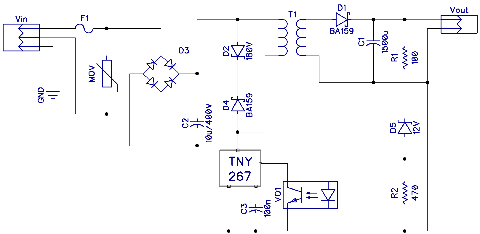
Step 3: Choose the Components
Once you have selected the topology for your switching power supply, it’s time to choose the components for your circuit. Select the right MOSFETs, diodes, capacitors, inductors, and control ICs based on your design requirements. Pay close attention to component ratings, thermal constraints, and efficiency considerations when selecting your components.
Step 4: Design the Circuit
With your requirements defined, topology selected, and components chosen, it’s time to design the circuit for your switching power supply. Lay out your components on a PCB, connect them according to your circuit design, and ensure proper grounding and signal paths. Consider factors such as noise, EMI, and thermal management in your circuit design.
Step 5: Test and Debug
Once your circuit is designed, it’s time to test and debug your switching power supply. Use a power supply tester or oscilloscope to measure the output voltage, current, and ripple of your circuit. Check for any anomalies or issues in your circuit and make necessary adjustments to ensure optimal performance.
Step 6: Fine-Tune Your Design
After testing and debugging your switching power supply, it’s time to fine-tune your design for optimal performance. Adjust component values, control loop parameters, and feedback mechanisms to optimize efficiency, stability, and transient response of your circuit. Continuously evaluate and improve your design based on testing results.
Conclusion
Designing a switching power supply can be a rewarding and challenging process. By following these steps and guidelines, you can design a high-performance and reliable switching power supply for your next project or product. Remember to continuously test, evaluate, and improve your design to achieve the best results.
Now that you have a better understanding of how to design a switching power supply, why not put your knowledge to the test and start designing your own circuit today?
Was this helpful?
0 / 0