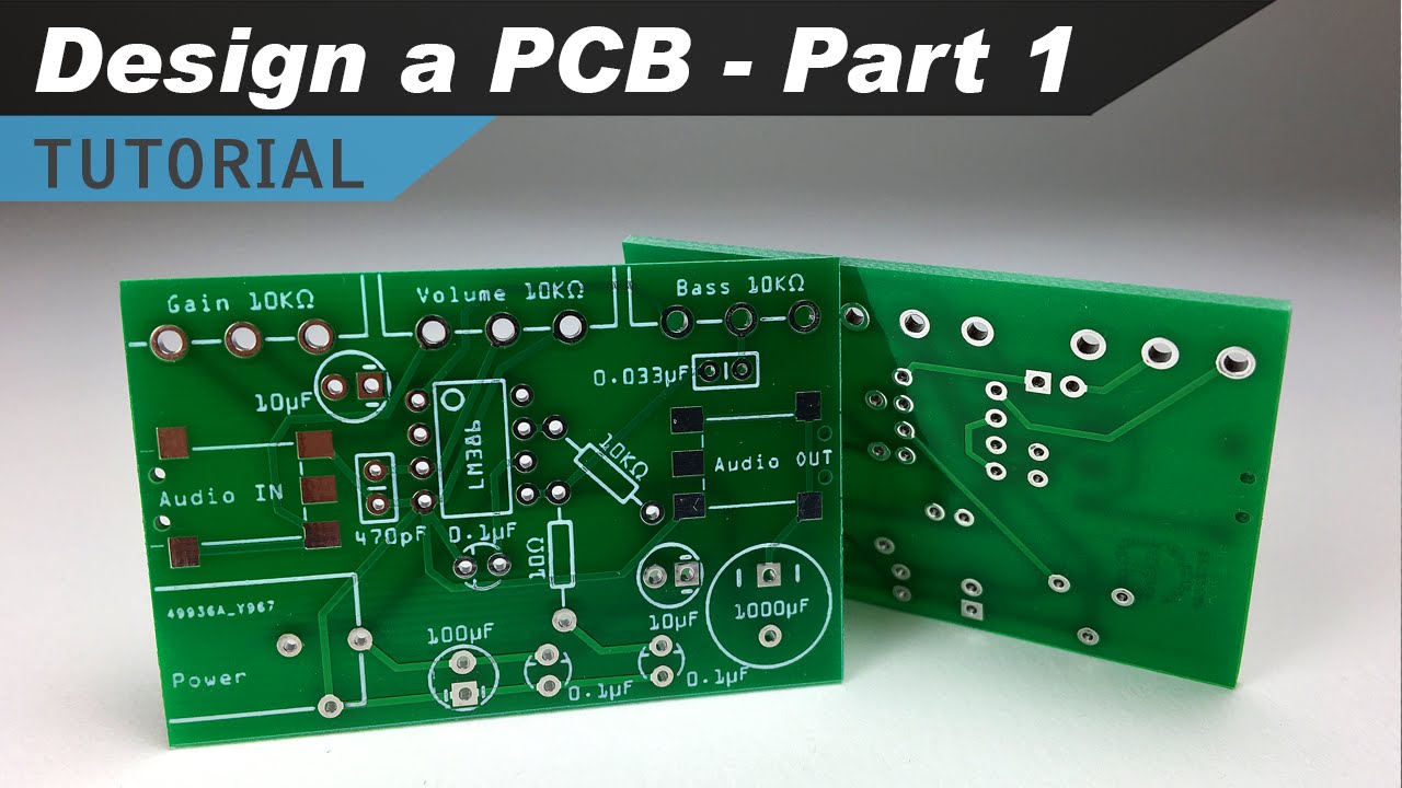
How to Create a PCB Layout
Creating a Printed Circuit Board (PCB) layout is a crucial step in the process of designing electronics. A well-designed PCB layout can greatly impact the performance and functionality of the final product. In this article, we will walk you through the steps to create a PCB layout that is both efficient and reliable.
Step 1: Schematic Design
The first step in creating a PCB layout is to design the schematic of your circuit. This involves drawing a diagram of the connections between components using a software tool such as KiCad or Eagle. The schematic provides a visual representation of how the components are connected and helps ensure that the circuit functions correctly.
Step 2: Component Placement
Once you have completed the schematic design, the next step is to place the components on the PCB layout. When placing components, consider factors such as signal integrity, thermal management, and ease of assembly. It is important to place components in a logical and organized manner to minimize noise and interference.
Step 3: Routing
Routing is the process of connecting the traces between components on the PCB layout. When routing, it is important to consider factors such as signal integrity, power distribution, and electromagnetic interference. Proper routing can help optimize the performance and reliability of the circuit.
Step 4: Ground Planes and Power Supplies
Ground planes and power supplies play a crucial role in the functionality of a PCB. Ground planes help provide a stable reference for the circuit, while power supplies ensure that components receive the correct voltage levels. Properly designing ground planes and power supplies can significantly improve the performance of the PCB layout.
Step 5: Design Rule Check
Before finalizing the PCB layout, it is important to perform a design rule check. This involves checking for errors such as trace width violations, clearance violations, and other design rule violations. By performing a design rule check, you can ensure that the PCB layout meets the required specifications and is ready for production.
Step 6: Prototyping and Testing
Once you have completed the PCB layout, it is important to prototype the circuit and test its functionality. Prototyping allows you to identify any potential issues or design flaws before moving to mass production. Testing the circuit ensures that it performs as expected and meets the required specifications.
Conclusion
Creating a PCB layout requires careful planning and attention to detail. By following the steps outlined in this article, you can create a PCB layout that is efficient, reliable, and meets the required specifications. Remember to consider factors such as schematic design, component placement, routing, ground planes, power supplies, design rule check, prototyping, and testing. With proper planning and execution, you can successfully create a PCB layout that will help bring your electronic design to life.
Was this helpful?
0 / 0